Scroll through the spec sheet of any modern camera or smartphone and you’ll quickly run into the term “backside-illuminated” — or its acronym BSI. It sounds like marketing jargon, but it describes a genuine change in how a CMOS image sensor is physically built. Understanding the difference between a frontside-illuminated (FSI) sensor and a backside-illuminated (BSI) sensor explains why your phone now shoots clean photos in dim restaurants — and why BSI has quietly become the default across almost every camera sold today.
How a Frontside-Illuminated (FSI) Sensor Works
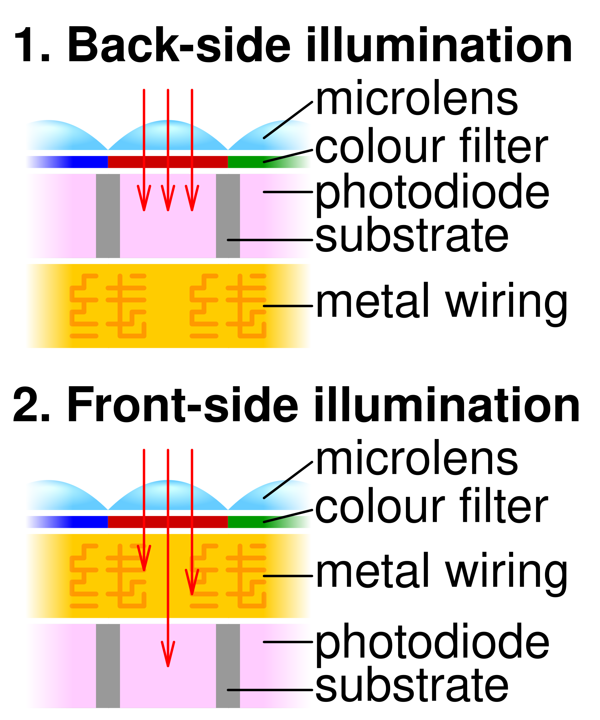
In a traditional CMOS sensor, each pixel is built as a layered stack on a silicon wafer. The photodiode — the light-sensitive region that converts photons into electrical charge — sits at the bottom of that stack. Above it lie the pixel’s transistors and several layers of metal wiring used to read the signal out. In a frontside-illuminated design, light enters from the top, so it has to travel through that wiring and circuitry before it ever reaches the photodiode.
That wiring is a problem. Metal interconnects reflect and absorb a meaningful share of the incoming photons, which lowers the sensor’s quantum efficiency (QE) — the fraction of photons that actually get converted into signal. Without help, an FSI sensor’s QE typically sits below 50%. Manufacturers partly compensate by adding microlenses (and sometimes “light pipes”) above each pixel to steer light around the metal, which can push peak QE up to roughly 80%. But those fixes add cost and complexity, and they work best only when light arrives straight on.
How a Backside-Illuminated (BSI) Sensor Works
A BSI sensor solves the problem by turning the chip around. The wafer is fabricated in much the same way, but the back of the silicon is then ground and etched away until only a few microns remain — thin enough to become transparent to light. The sensor is then flipped so that light enters through this freshly thinned backside and strikes the photodiode directly, with no wiring in the way.
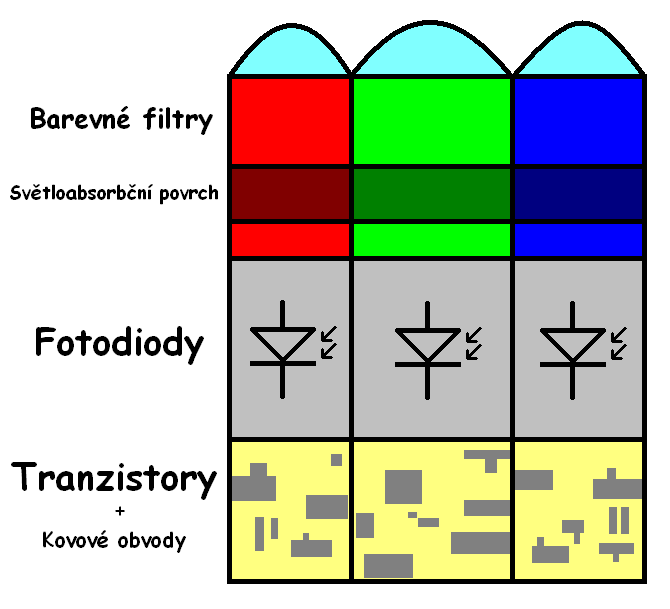
The payoff is dramatic. With the metal stack moved out of the optical path, a well-made BSI sensor can achieve quantum efficiency above 90%, and it does so across a wider range of wavelengths — including the blue and ultraviolet end of the spectrum, where FSI sensors traditionally struggle. BSI sensors also exhibit less optical crosstalk (light bleeding between neighboring pixels), which helps preserve sharpness and color accuracy.
Why BSI Wins on Low Light
More captured photons mean a stronger signal relative to the sensor’s electronic noise. In practical terms, BSI CMOS is often described as being roughly one f-stop better in low light than a comparable FSI design: a BSI chip shows about as much noise at ISO 12800 as an FSI chip does at ISO 6400. That’s a meaningful jump for a phone camera with a tiny sensor — the main reason BSI took over smartphones first.
The geometry also helps lens design. Because a BSI pixel can accept light from a wider angle, manufacturers can pair it with a brighter, larger aperture and a shorter, lower-profile lens stack without the corner shading and vignetting that can plague FSI sensors behind wide lenses.
The Cost of Flipping the Chip
None of this comes free. Thinning a wafer to a few microns — uniformly, across the entire surface, without damaging the photodiode — is a delicate and expensive process. The thinned layer must be defect-free and of even thickness, or sensitivity varies across the frame. BSI sensors also need a carefully engineered anti-reflection and surface-passivation layer, and their very thin silicon initially made them more prone to color crosstalk at small pixel sizes — a problem manufacturers have had to engineer around.
That’s why BSI started life in niche, high-end applications. Sony commercialized the first mass-market BSI CMOS sensor under the Exmor R brand in 2008–2009, appearing first in compact camcorders. The technology reached smartphones with devices like the Apple iPhone 4 in 2010 and spread from there. Today BSI is standard in phones and mainstream interchangeable-lens cameras from Sony, Canon, Nikon, and Fujifilm, with the added complexity now absorbed into normal production costs.
BSI vs FSI at a Glance
- Light path: FSI light passes through metal wiring; BSI light reaches the photodiode directly.
- Quantum efficiency: FSI typically below 50% (up to ~80% with microlenses); BSI often above 90%.
- Low-light performance: BSI is roughly one f-stop better than FSI.
- Spectral range: BSI is more sensitive in blue and UV; FSI is weaker there.
- Manufacturing: FSI is simpler and cheaper; BSI requires precise wafer thinning and costs more.
Which One Should You Care About?
For most buyers the honest answer is: you rarely need to choose. BSI has won the mainstream, and nearly every current smartphone and modern mirrorless camera uses it. Where the distinction still matters is in the details — a BSI sensor is a genuine advantage for handheld low-light work, and its wider light-acceptance angle lets designers pair it with brighter lenses. FSI, meanwhile, still appears in some cost-sensitive and industrial designs where its simpler, cheaper fabrication makes sense and light is plentiful.
Conclusion
Backside illumination is not a marketing label — it’s a structural change that removes the sensor’s own wiring from the path of incoming light. The result is more photons captured per pixel, better low-light performance, and a wider spectral response, at the cost of a harder manufacturing process. That trade-off has already been paid, which is why BSI now sits inside the camera you carry every day.
FAQ
Does BSI matter more on small sensors?
Yes. The benefit is most visible on smartphones and compact cameras, where pixels are tiny and every photon counts. On large full-frame sensors the relative gain is smaller, though BSI still helps edge and corner performance.
Is BSI the same as stacked CMOS?
No. BSI describes which side of the silicon receives light. Stacked CMOS is a separate technique that moves processing circuitry onto a second, bonded die — most stacked sensors are also BSI, but the two ideas solve different problems.
Are all modern cameras BSI?
Almost all smartphones and most current mirrorless cameras use BSI sensors. A few entry-level and industrial cameras still use FSI to keep costs down.
Related Posts

Global Shutter vs Rolling Shutter: What’s the Difference and Why It Matters
Every digital camera turns light into an image using a…
How Autofocus Works: Phase Detection vs Contrast Detection
Every time you half-press the shutter button, your camera has…

Weather Sealing in Cameras Explained: IP Ratings, Seals & Limits
"Weather sealing" is one of the most heavily marketed —…