
What Is a Stacked CMOS Sensor?
A stacked CMOS sensor is a type of image sensor in which the light-capturing pixel layer and the signal-processing circuitry are built on separate silicon chips and then bonded together, one on top of the other. In a conventional CMOS sensor, the photodiodes and the readout circuits sit side by side on the same piece of silicon. Stacking moves that circuitry onto a dedicated layer directly beneath the pixels, freeing up space and opening the door to dramatically faster readout speeds, more powerful on-chip processing, and smaller camera modules.
The idea sounds simple, but it required serious semiconductor manufacturing know-how. Sony, which has led the field from the start, first commercialized a stacked CMOS image sensor in 2012 under the “Exmor RS” brand. Since then, stacked sensors have gone from smartphone camera modules to flagship full-frame mirrorless cameras and industrial machine-vision systems.
How Stacking Works
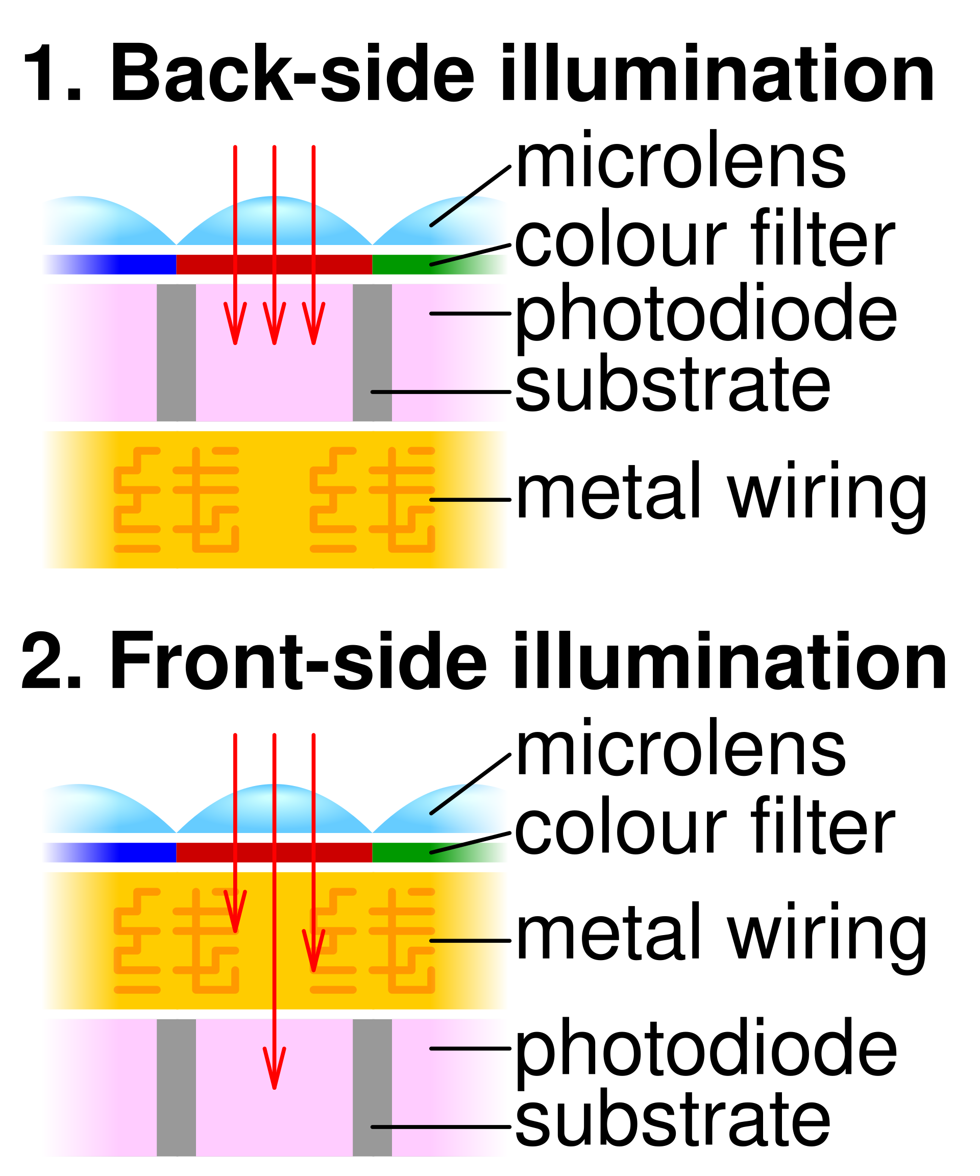
To understand stacking, it helps to know one more term: back-illuminated, or BSI, design. In a traditional front-illuminated sensor, the wiring layer sits between the incoming light and the photodiode, absorbing some of the light. A back-illuminated sensor flips the structure so light reaches the photodiode directly, with the wiring moved behind it — improving sensitivity, especially in low light.
Stacked sensors build on that. A conventional BSI sensor still needs a supporting substrate, and the readout and signal-processing circuits live around the edges of the pixel array. In a stacked design, that support substrate is replaced by a fully functional logic chip containing the image-processing circuits. The back-illuminated pixel layer is bonded on top of it, and the two communicate through high-density interconnects. The result is a sensor where the pixels do one job — catching light — while a dedicated layer underneath does the heavy lifting of reading, converting, and processing that data.
Why Stacking Matters: Speed, Size, and Function
The headline benefit is speed. Because the processing circuits now have their own dedicated silicon with room to expand, a stacked sensor can read its pixels far faster than a conventional design. That speed shows up in real-world shooting in a few concrete ways:
- Less rolling-shutter distortion. Fast readout shortens the time gap between reading the top and bottom of the frame, so fast-moving subjects — a golf swing, a passing train, a panning shot — show less of the “jello” skew typical of electronic shutters.
- Faster burst shooting and video. Flagship cameras with stacked sensors can shoot at 20, 30, or even 120 frames per second with autofocus and auto-exposure tracking, and record high-frame-rate video that older sensors could not.
- More room for extra features. The logic layer can carry image-plane phase-detection autofocus, HDR processing, noise reduction, and even onboard memory. Sony’s three-layer stacked sensor, announced in 2017, added a DRAM layer so a sensor could read a 19.3-megapixel image in 1/120 second and shoot super slow-motion video at up to 1,000 frames per second.
- Smaller modules. Because circuitry no longer competes with pixels for space, stacked sensors let manufacturers fit bigger, higher-resolution sensors into thinner smartphones.
From Smartphones to Full-Frame: Key Milestones
Sony shipped the first Exmor RS stacked sensors into smartphones and tablets in 2012 and 2013. The technology scaled up quickly. The Sony α9, launched in 2017, was the first full-frame mirrorless camera built around a stacked CMOS sensor with integral memory — a 24.2-megapixel sensor with roughly 20 times the readout speed of a conventional full-frame sensor, enabling 20 fps continuous shooting, blackout-free viewfinder performance, and electronic shutter speeds up to 1/32000 second.
The technology kept evolving in both directions. For industrial and machine-vision use, Sony’s “Pregius S” technology combined a stacked structure with a global-shutter, back-illuminated pixel design to deliver distortion-free imaging with pixels as small as 2.74 μm. In 2025, Sony announced the IMX927, a stacked sensor with about 105 effective megapixels and output up to 100 fps for advanced inspection systems. Meanwhile, stacked sensors remain the standard in premium smartphones, powering fast autofocus, HDR, and slow-motion video in a package just a few millimeters thick.
Stacked vs. Conventional and Back-Illuminated Sensors
It is worth untangling the three terms, because they are often mentioned together and describe different things:
- Front-illuminated (conventional): the original layout, with wiring in front of the photodiodes. Lowest sensitivity of the three, and the slowest readout.
- Back-illuminated (BSI): wiring moved behind the photodiodes for better light capture. Improves image quality, but readout circuits still share space with the pixel array.
- Stacked: the BSI pixel layer is bonded on top of a separate logic chip. This is a structural change that primarily buys speed and functionality rather than light sensitivity alone.
In practice, modern stacked sensors are almost always back-illuminated as well, combining the sensitivity advantage of BSI with the speed advantage of stacking.
What Stacked CMOS Means for You
If you shoot action, sports, wildlife, or anything that moves quickly, a stacked sensor is one of the most meaningful upgrades you can get — it is the technology behind the silent, blackout-free bursts and low-distortion electronic shutters in today’s flagship cameras. For smartphone users, it is largely invisible: it is why your phone can lock focus instantly, capture HDR without a shutter lag, and record slow-motion clips that were unthinkable a decade ago. For engineers and machine-vision integrators, stacking is what makes high-resolution, high-frame-rate, distortion-free inspection possible in ever-smaller packages.
The trend is only accelerating. As stacked designs add more layers — DRAM for buffering, AI processing for on-sensor intelligence — the humble image sensor is becoming a complete camera system on a chip, and the gap between what a sensor “sees” and what it “computes” keeps shrinking.
Conclusion
Stacked CMOS sensors are a quietly revolutionary idea: split the sensor’s two jobs — sensing light and processing it — onto separate silicon layers, then stack them. That one structural change unlocked the speed, compactness, and on-chip intelligence that define modern photography, from the super-slow-motion video in your pocket to 20 fps blackout-free bursts on a full-frame camera. The next time you freeze a moment that would have blurred a decade ago, a stacked sensor is likely the reason.
FAQ
What is the difference between stacked and back-illuminated CMOS sensors?
Back-illuminated (BSI) design moves the wiring behind the photodiodes to improve light sensitivity. Stacking is a separate structural change: it bonds the pixel layer on top of a dedicated signal-processing chip to increase readout speed and add functionality. Most stacked sensors are also back-illuminated.
Does a stacked sensor improve image quality?
Its main advantage is speed, not raw image quality — that speed reduces rolling-shutter distortion and enables faster bursts and video. Image quality benefits mainly come from the back-illuminated structure that most stacked sensors also use.
Which cameras use stacked CMOS sensors?
Sony pioneered them and uses them in cameras like the α9 series; the technology has since spread across flagship mirrorless cameras from multiple brands and is standard in premium smartphone cameras.
Related Posts
Backside-Illuminated (BSI) vs Frontside-Illuminated Sensors: What’s the Difference?
Scroll through the spec sheet of any modern camera or…
High-Resolution Camera Technology 2026: From 200MP Sensors to Computational Photography
In 2026, "more megapixels" no longer means "a better camera."…
Mirrorless Camera Design: How Removing the Mirror Changed Cameras
For most of the twentieth century, the single-lens reflex (SLR)…