Flip over almost any modern camera or smartphone and the spec sheet will advertise a “BSI” or “back-illuminated” sensor. The name sounds technical, but the idea behind it is surprisingly simple: BSI is a physical rearrangement of the sensor’s internal layers that lets more light reach each pixel. It is not a brand, a filter, or a processor feature — it is geometry. And that one change in geometry is a big part of why cameras became dramatically better in low light over the last fifteen years.
The Problem with Front-Illuminated Sensors
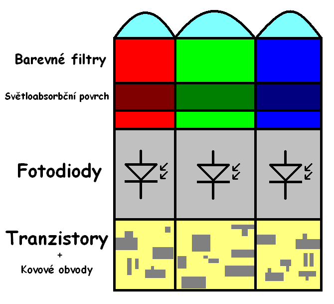
A traditional CMOS sensor is built like a layered sandwich that light enters from the front. From the top down, the layers are the microlens, the color filter, the metal wiring, and finally the photodiode that actually converts photons into electrical charge. Notice the problem: the wiring sits in front of the photodiode.
Those metal traces are what read the signal out of each pixel, and they are not transparent. In a “front-illuminated” (FSI) design, some of the incoming light bounces off the wiring or is absorbed before it ever reaches the photodiode. On a large sensor this loss is tolerable, because each pixel is big enough that the wiring only shadows a small fraction of it. On a small sensor, it is a real handicap — the wiring occupies a proportionally much larger share of every tiny pixel.
How a Back-Illuminated Sensor Works
A back-illuminated sensor contains exactly the same components, but flips their order. During manufacturing, the silicon wafer is turned over and its back side is ground down until it is only a few micrometers thick. Light then enters through this thinned back side and strikes the photodiode first, with the wiring moved behind it and out of the light path.
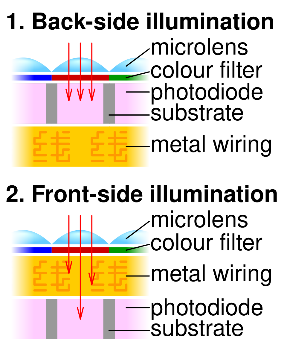
The payoff is measurable: the chance that an incoming photon gets captured rises from roughly 60% in a front-illuminated design to over 90% in a back-illuminated one — a gain of about half a stop of light. The improvement is largest where pixels are smallest, which is precisely why BSI became a phone-sensor technology first.
Why Small Pixels Benefit the Most
BSI matters most when pixels are small because that is where the wiring steals the biggest share of the light. Phone sensors pack millions of pixels into a chip the size of a fingernail, with individual pixels measuring around a single micron across. Moving the wiring behind the photodiode is what allowed those pixels to keep shrinking while still gathering enough light to produce clean images.
Sony brought the idea to consumers first, announcing its “Exmor R” back-illuminated sensor in June 2008 and claiming nearly twofold sensitivity versus its front-illuminated predecessor. Those sensors soon found their way into phones — including Apple’s iPhone 4S, which used a Sony-built BSI sensor — while OmniVision mass-produced its own “OmniBSI” line for a long list of handsets. Samsung’s ISOCELL phone sensors are BSI designs too, adding physical barriers between pixels to further reduce crosstalk and color bleeding.
From BSI to Stacked Sensors
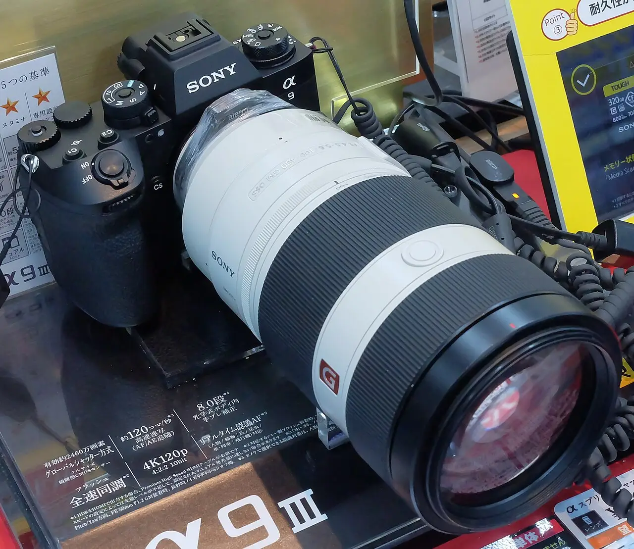
BSI solved the light-path problem; the next bottleneck was speed. A “stacked” sensor takes the BSI idea a step further by bonding the photodiode layer to one or more separate layers of logic and memory below it. Sony announced the first stacked CMOS sensor in January 2012, claiming roughly 30% more light captured plus dramatically faster readout. That extra circuitry is what lets today’s speed-focused flagships — like the Sony a9 III, Sony a1, and Nikon Z9 — fire off huge bursts and read the sensor fast enough to suppress rolling-shutter distortion. Almost every modern stacked sensor is also back-illuminated, so the two technologies usually arrive together.
BSI in the Cameras You Buy Today
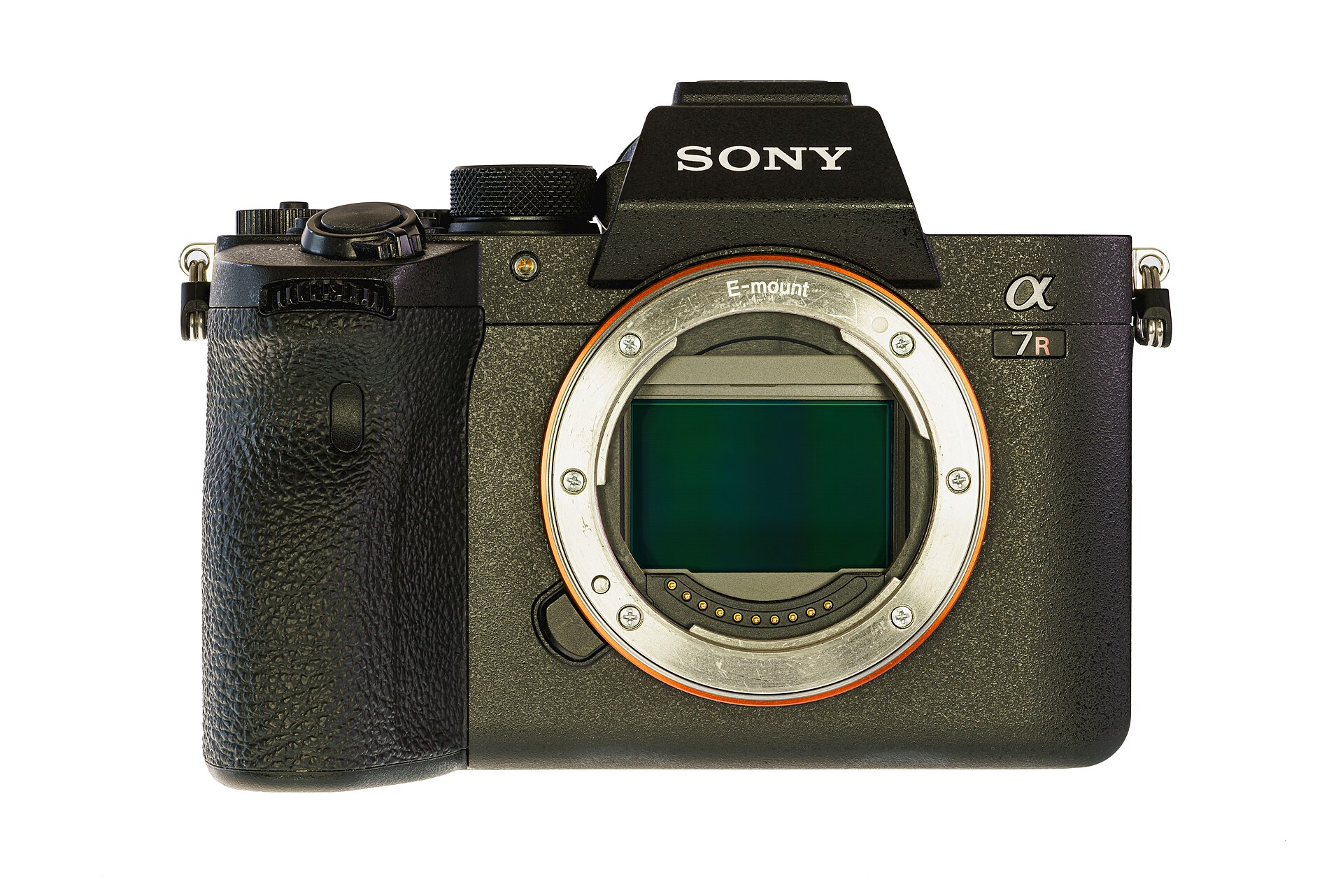
Back-illumination has quietly become the default. Full-frame BSI arrived in 2015 with the Sony a7R II, and today most interchangeable-lens cameras, nearly all smartphones, and even security and automotive cameras use BSI or BSI-stacked sensors. When a spec sheet lists “BSI CMOS”, “back-side illuminated”, or “stacked”, it is describing this same family of technologies — wiring moved out of the light’s way, and often the supporting circuitry stacked beneath the pixels.
Conclusion
Back-illuminated sensors are one of the quiet revolutions in digital imaging: a simple flip of the silicon that put the photodiode first and the wiring behind it. That one change unlocked cleaner low-light photos from ever-smaller pixels and paved the way for the stacked sensors that power today’s fastest cameras. The next time you see “BSI” on a spec sheet, you will know exactly what it means — and why it matters.
FAQ
Is a BSI sensor always better than an FSI sensor? In low light and in small-pixel designs, yes — BSI captures meaningfully more light. On very large pixels the advantage narrows, but modern BSI processes also reduce dark current, so there is rarely a downside today.
Does BSI change resolution or sharpness? Not directly. BSI affects how much light each pixel collects (sensitivity and noise), not the megapixel count. Sharper per-pixel results come mainly from the lens and other processing.
What is the difference between BSI and a stacked sensor? BSI moves the wiring behind the photodiode. A stacked sensor goes further and bonds the photodiode layer to separate logic and memory layers beneath it, mainly to boost readout speed. Stacked sensors are almost always back-illuminated as well.
Are all modern cameras BSI? Most phones and many dedicated cameras are, but not all. Some larger, lower-cost sensors still use front-illuminated designs where the cost and light-loss tradeoffs are acceptable.
Related Posts
Global Shutter vs Rolling Shutter Explained: Why the Sony a9 III Changed the Game
Nearly every digital camera you've ever used — from your…
High-Resolution Camera Technology 2026: From 200MP Sensors to Computational Photography
In 2026, "more megapixels" no longer means "a better camera."…
Electronic vs Mechanical Shutter: Which Should You Use?
Every photograph depends on one small but critical decision: how…